
Mengxia Liu: New Materials for the Semiconductor Industry

Mengxia Liu, the newest faculty member in Yale’s Department of Electrical Engineering, is on a pursuit to create more efficient solar cells and smart sensors by developing novel materials. Liu, who completed her Ph.D. at the University of Toronto in 2019, has an extensive background in semiconductor fabrication and characterization, which she will use to study the properties of novel semiconducting materials.
 As Liu puts it, solar energy is “an important topic” – in 2005, motivated by the constant climb in global temperatures, Congress passed the Energy Policy Act, promising a 30% investment tax credit for residential and commercial solar energy systems. The Energy Policy Act, one of the first policies addressing solar energy, sparked a renewed interest in the commercialization of solar energy among scholarly communities.
Researchers began to study the materials, as well as manufacturing processes, surrounding photovoltaic (PV) cells. In a PV cell, a negatively charged and positively charged silicon layer sandwich a junction. When sunlight strikes the surface of these cells, photons distribute energy to electrons, causing them to move from the negatively charged to the positively charged layer. If an external wire is connected between the layers, electrons flow back to the negatively charged layer, generating electricity. Beyond the solar industry, PV cells also have applications in other energy storage and electronic technologies, such as batteries and computer chips. When Liu started her Ph.D. studies in 2014, new materials had emerged, expected to be cheaper and easier to manufacture compared to silicon - the leading material in the photovoltaic market.
In her doctoral career at the University of Toronto, Liu studied the synthesis and fabrication process of PV cells, in particular, the quantum dot based solar cells. Quantum dots are semiconducting nanocrystals that have a size of several nanometers. Four years into her program, she began to study the surface engineering of quantum dots, making them compatible with a variety of organic or inorganic materials, and fabricating efficient solar cell devices that can compensate the absorption of silicon. Though the engineering processes were well understood, Liu realized that the physical picture behind energy conversion and charge transport in real devices is lacking.
“That’s the hurdle against the speed of discovery of new materials and the generation of new device concept,” said Liu. “A better understanding of the mechanisms behind charge transport and dynamics, as she saw, could generate research breakthroughs in semiconductor research.”
After completing her Ph.D. in 2019, Liu took on a postdoctoral opportunity at the University of Cambridge, where she developed novel techniques to better understand how energy carriers behave in real time. She combined two preexisting technologies - transient absorption spectroscopy and optical microscopy - to map the flow of energy in space with an extremely high temporal resolution.
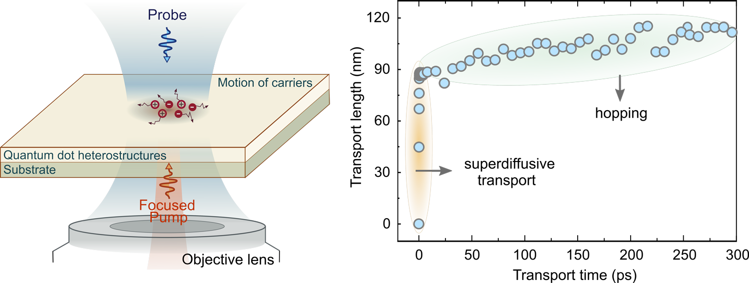 Liu’s technique can be compared to producing dynamic videos from static photographs – when Liu compiled different energy measurements, she was able to show the transport of charges across hundreds of femtoseconds.
“We can couple the information in space and time in one measurement to investigate how the carriers are moving inside the material and across the grain boundaries,” said Liu. “With this technique, we are able to investigate the charge transport mechanisms of these materials at the very early stage after photoexcitation – for instance, we focused on the scope of several hundreds of femtoseconds, when charges move in an unconventional way.”
In her lab - within the Energy Sciences Institute at Yale’s West Campus - Liu will explore novel electronic materials for efficient solar cells, light sources, and photodetectors. Within her future research, Liu will investigate different heterostructures – by incorporating semiconductors of different types – to improve energy efficiency. Different combinations of materials, Liu believes, enable synergistic phenomena, generating new physical properties that are inaccessible to a single materials platform.
 “One example we explored earlier is the integration of quantum dots and metal halide perovskites, two types of solution-processed semiconductors,” Liu said. “Quantum dots can absorb and emit in the infrared, but they have poor charge transport properties. Perovskites, on the other hand, are vice versa. They have very good electronic conductivity, but don't have a response in the infrared. The idea was, by combining these two materials, to produce a hybrid system that has both good charge mobility but also infrared responsivity.”
Liu noted that the cutting-edge materials science, microelectronics, and physics research found in the different SEAS departments were what drew her to join the electrical engineering faculty. She plans to collaborate with others across SEAS to gain molecular-level understandings of the solution-processed materials and hybrid interfaces, photophysical understandings of operando electronic devices, and eventually, continue to shape the field of semiconductor device manufacturing.
“Right now, the semiconductor industry is pushing to get new materials for photovoltaics to utilize solar energy in a more efficient way,” Liu said. “Industry and governmental organizations are putting a lot of effort and investment in that direction. I believe the way that we produce and use electricity will change significantly in the next decade, especially when we’re moving away from fossil fuels to other new types of energy sources.”
Beyond photovoltaics, semiconductor devices in general will become cheaper, smarter, more energy-efficient, and can be integrated in the future, especially with the implementation of the CHIPS Act of 2022. This requires the development of novel electronic materials beyond silicon to improve the efficiency and reduce the energy consumption of communications and computation systems.”
Kevin Pataroque (He/Him/His) is a second year Environmental Engineering Ph.D. student in the Elimelech Lab. A recent graduate of Case Western Reserve University, Kevin seeks to make scientific research accessible and relevant beyond the laboratory. His research areas include desalination processes, membrane technology, and clean water equity.