A Breakthrough in Molding Materials at the Nanoscale
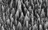
In recent years, researchers have made advances in molding metals and alloys at the nanoscale level. But the ability to mold a coveted class of materials known as ordered phases at that scale has been elusive.
In a potential game-changing shift in how nano- and quantum devices are designed and manufactured, researchers in the lab of Jan Schroers, professor of mechanical engineering & materials science, have discovered that these materials are actually very conducive to nanomolding, thanks to their atoms’ ability to self-organize. The breakthrough could lead to new uses for ordered phases, which make up the large majority of functional materials, including superconductors, topological insulators, and quantum materials. The results are published today in Physical Review Letters.
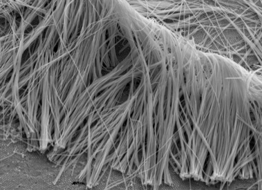
When the researchers first started nanomolding amorphous metals about 10 years ago, they were encouraged by the possibilities, albeit with some reservations. “It was pretty exciting, and you could make some really nice catalysts,” Schroers said. “But there was a limitation in that you could only do a few alloys out of the billions and billions of alloys.”
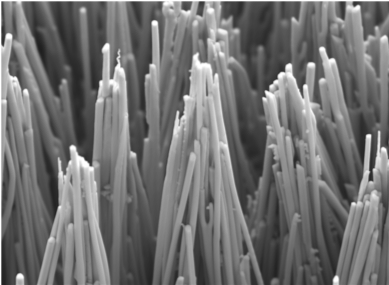
Then the researchers discovered that atomic diffusion, in which a change in pressure transports the atoms, would allow them to efficiently mold crystalline metals. In addition, decreasing the size of the mold actually made the process easier. But there were still drawbacks. The composition of the molded nanostructure varied uncontrollably, and because ordered phase materials are made up of atoms of different sizes moving at different speeds, it seemed that nanomolding would force the atoms out of order - and that would result in a different material lacking the desired functional properties.
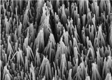
Recently, though, they discovered that they could control the composition of these materials. Working with Naijia Liu, a grad student in Schroers’ lab and lead author of the study, Schroers found that a broad range of ordered phase materials can be shaped by using a process that they called thermo-mechanical nanomolding. It involves pressing the material down into a nanomold at temperatures well below the melting temperature, and creating wires with diameters as small as 10 nm — 10,000 times smaller than a human hair. Also – and very surprising - the entire nanowire is one crystal, a requirement for most functional applications of electronic materials. The wires they created featured a wide range of crystal structures and properties, including superconductors, topological crystalline insulators, and phase change materials.
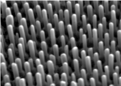
They attribute the ability to precisely maintain the composition and place each atom species precisely on its position to a property of ordered phase materials that forces their atoms to self-organize into its specific structure and chemistry. That’s because the atoms of the faster-moving component are unable to occupy the positions the slower-moving counterparts desire to occupy.
“So now, all these functional materials can be molded in this very controlled way,” Schroers said. “It’s really interesting, technologically, to explore these complicated materials with this method.”
In addition to Schroers and Liu, the paper's authors are Yujun Xie, Guannan Liu, Sungwoo Sohn, Arindam Raj, Guoxing Han, Bozhao Wu, Judy J. Cha, and Ze Liu.

